0505A


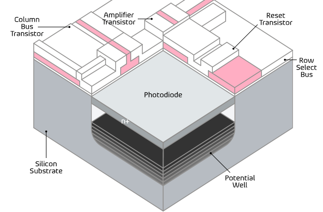
CMOS Technology Advantage
<
- Choice of various scintillator
- Provide resolution requirements based on work condition
- Provide optimized Sensitivity
- Radiation hard pixel design with adjustable saturation dose levels
- Suitable for all industrial applications
- Clear image with high-resolution and low noise performance
More precise details even
at Smallest components
at Smallest components
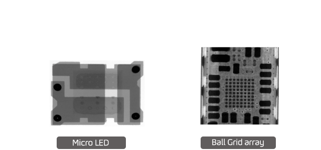
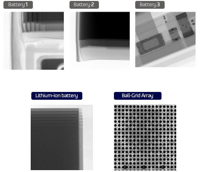
- More precise NDT inspections for even the smallest components
- Industrial X-ray is ideal for
- Solder inspection, Electronics inspection, Battery inspection Ball Grid Array inspection, Through Hole Technology inspection
Excellent High-Resolution
by CMOS Technology
by CMOS Technology
- Standard models in a range of pixel and detector sizes
- Robust mechanical design
Application


Specification
| Sensor Type | CMOS |
|---|---|
| Scintillator | CsI / GOS |
| Total Pixel Matrix (Pixels) | 1176 x 1104 (@1x1) |
| Active Area (mm) | 58 x 54 |
| Pixel Pitch (㎛) | 49.5 (@1x1) |
| Frame Rate (fps) | 30 (@1x1) |
| Energy Range (kVp) | 40 ~ 160 |
|---|---|
| Power Consumption | 24 V / 3.54 A |
| A/D Conversion (bits) | 14 |
| Data Interface | GigE / C-link |
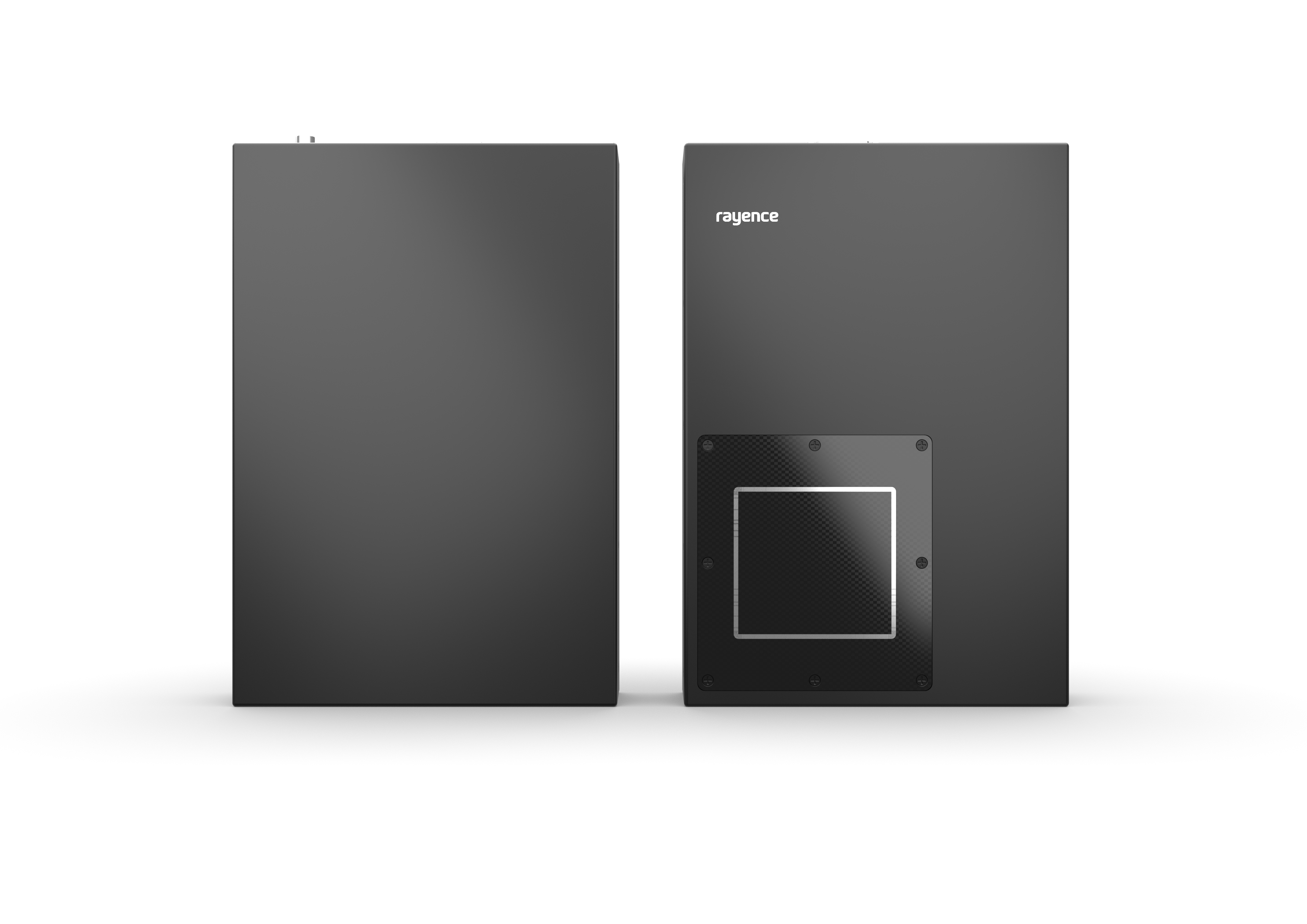
| Dimension (mm) | 146.0 x 214.0 x 33.7 |
| Weight (kg) | 1.9 |
- Product design and specifications are subject to change without prior notice to improve product performance.
- Downloads are only supported for customers who have filled out information.
- The image quality level may vary depending on the product usage environment.

- Averaging : Remove the noise of image
- Blending : Confirming the difference between levels
- Line profile : Available to Image validation based on ASTM Standard.